Product Summary
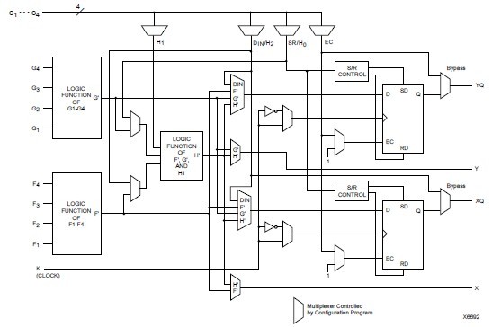
The XC4028EX-4PG299I is implemented with a regular, flexible, programmable architecture of Configurable Logic Blocks (CLBs), interconnected by a powerful hierarchy of versatile routing resources, and surrounded by a perimeter of programmable Input/Output Blocks (IOBs). They have generous routing resources to accommodate the most complex interconnect patterns. The XC4028EX-4PG299I is customized by loading configuration data into internal memory cells. The FPGA can either actively read its configuration data from an external serial or byte-parallel PROM (master modes), or the configuration data can be written into the FPGA from an external device (slave and peripheral modes). XC4028EX-4PG299I FPGA is supported by powerful and sophisticated software, covering every aspect of design from schematic or behavioral entry, floor planning, simulation, automatic block placement and routing of interconnects, to the creation, downloading, and readback of the configuration bit stream.
Features
XC4028EX-4PG299I features: (1)Fully PCI compliant (speed grades -2 and faster); (2)Abundant flip-flops; (3)Flexible function generators; (4)Dedicated high-speed carry logic; (5)Wide edge decoders on each edge; (6)Hierarchy of interconnect lines; (7)Internal 3-state bus capability; (8)Eight global low-skew clock or signal distribution networks; (9)System Performance beyond 80 MHz; (10)Flexible Array Architecture; (11)Low Power Segmented Routing Architecture; (12)Backward Compatible with XC4000 Devices.
Diagrams

 |
 XC4000 |
 Other |
 |
 Data Sheet |
 Negotiable |
|
||||
 |
 XC4000A |
 Other |
 |
 Data Sheet |
 Negotiable |
|
||||
 |
 XC4000E |
 Other |
 |
 Data Sheet |
 Negotiable |
|
||||
 |
 XC4000H |
 Other |
 |
 Data Sheet |
 Negotiable |
|
||||
 |
 XC4000X |
 Other |
 |
 Data Sheet |
 Negotiable |
|
||||
 |
 XC4000XL |
 Other |
 |
 Data Sheet |
 Negotiable |
|
||||
 (China (Mainland))


